
Leadframes Market Demand, Size & Forecast by 2034
Coverage: by Type (Stamping Process Lead Frame, Etching Process Lead Frame, Others); Substrate Material (Copper, Iron-Nickel Alloy, Aluminum, Others); Layer (Single-Layer, Multi-Layer); Application (Integrated Circuit, Discrete Device, Others); Industry Vertical (Automotive, Consumer Electronics, Telecommunications, Aerospace & Defense, Others); and Geography (North America, Europe, Asia Pacific, and South and Central America)
- Status : Data Released
- Report Code : TIPTE100000452
- Category : Electronics and Semiconductor
- No. of Pages : 150
- Available Report Formats :


- Last update date : October 22, 2026


2025 Market Size
US$ 78.85 Bn
Base year value
2034 Forecast
US$ 259.37 Bn
Projected by 2034
CAGR 2026-2034
14.15 %
Growth rate
Addressable Market
US$ 1,457.08 Bn
(2026-2034)
The Leadframes Market was valued at US$ 78.85 Billion in 2025 and is projected to reach US$ 259.37 Billion by 2034, registering a CAGR of 14.15% during 2026–2034. Expansion is supported by semiconductor packaging demand, increasing electronic content in vehicles, and rising requirements for compact, thermally efficient packages. Growth is also shaped by precision manufacturing, advanced plating, and greater use of leadframes in power, analog, and mixed-signal semiconductor devices.
Increasing semiconductor manufacturing activity is strengthening the Leadframes Market size across North America, where automotive electronics, industrial automation, and reshoring of semiconductor packaging capacity are supporting demand. The region is estimated to register a CAGR of 11.8–12.6% between 2026–2034. Investments in domestic semiconductor ecosystems, advanced packaging, and automotive semiconductor supply chains should support regional consumption of precision leadframes.
Leadframes Market Assessment and Insights
- North America: North America held an estimated 18–22% Leadframes Market share in 2025 and is projected to grow at a CAGR of 11.8–12.6% between 2026–2034, supported by semiconductor capacity expansion, automotive electronics, and localized packaging.
- US: The US represented approximately 72–76% of North American demand in 2025 and is expected to expand at a CAGR of 11.6–12.4% during 2026–2034, driven by semiconductor investment and advanced packaging.
- Europe: Europe accounted for approximately 15–19% share in 2025 and is projected to register a CAGR of 12.0–12.8% through 2034, with Germany, France, Italy, the UK, and Spain supporting automotive and industrial semiconductor demand.
- Asia Pacific: Asia Pacific represented approximately 48–52% share in 2025 and is expected to record a CAGR of 14.8–15.6% during 2026–2034, led by China, Japan, South Korea, Taiwan, and Southeast Asian production hubs.
- Largest Segment: Stamping Process Lead Frame held an estimated market share of 57–61% in 2025, expanding at a CAGR of 13.8–14.4% during 2026–2034 due to high-volume production economics.
- High Growth Segment: Automotive accounted for approximately 20–24% share in 2025, with a projected CAGR of 16.0–16.8% during 2026–2034, supported by EVs, ADAS, power management, and vehicle electrification.
- Key companies analyzed in detail: NINGBO HUALONG ELECTRONICS CO., LTD.; Precision Micro; ENOMOTO Co., Ltd.; Veco Precision Metal; SHINKO ELECTRIC INDUSTRIES CO., LTD.; Sumitomo Metal Mining Co., Ltd.; Hitachi Cable, Ltd.; STATS ChipPAC Ltd.; Amkor Technology, Inc.; Mitsui High-tec, Inc.
Source: The Insight Partners' analysis based on proprietary research, government publications, company annual reports, investor presentations, industry databases, and expert interviews.
Lead frames have moved beyond their traditional application as basic carriers for packages to being highly developed elements that require precise manufacturing with regard to thickness, fine pitch structure, stamping/etching procedures, and special surface finishes. Future growth will be associated more and more with miniaturization, thermal/electrical management considerations, and semiconductors. Copper plays an important role in relation to conductivity and thermal management, but better plating processes and designs can contribute to addressing higher performance expectations at the level of package.
The future growth of the Leadframes Market will be driven by Asia Pacific, while localized semiconductor production in North America and Europe will provide additional opportunities for regional growth. Developments in the sphere of automotive electrification, industrial automation, telecommunication infrastructure, and power electronics will continue providing steady demand for package interconnects. Advanced packaging and semiconductor ecosystems investments may provide additional push for market regionalization.
Leadframes Market Report Scope
| Report Attribute | Details |
|---|---|
| Market size in 2025 | US$ 78.85 Billion |
| Market Size by 2034 | US$ 259.37 Billion |
| Global CAGR (2026 - 2034) | 14.15% |
| Historical Data | 2021-2024 |
| Forecast period | 2026-2034 |
Leadframes Market Analysis
The requirement for lead frames has been created by semiconductors assembly, ICs, discrete devices, power electronics, sensors and automobile electronics. The development of the Leadframes Market has been made possible with the help of a value chain comprising of copper and alloy producers, precision strip producers, tool producers, stamper/etcher producers, platers, semiconductor packaging companies and device producers. Material selection is critical for conductivity, mechanical properties, thermal properties and reliability.
Supply dynamics in the Leadframes Market will be dependent on tooling, automation, surface finishing, dimensional tolerances, and yield. Stamping will be better for large volumes while etching will allow for intricate designs. Semiconductor firms usually qualify their suppliers over a long period since dimensional tolerance and plating are important for package yields. Hence, capacity will go to manufacturers with specific capabilities.
The Leadframes Market competition includes the integration of the packaging firm and the leadframe manufacturers. While SHINKO ELECTRIC INDUSTRIES CO., LTD. is a company that integrates stamping, etching, plating, and semiconductor packaging, Mitsui High-tec, Inc. focuses on precision manufacture and electronics products that are used in automobiles. On the other hand, Amkor Technology, Inc. is a company that deals with offering a wide array of leadframe packaging services, which makes an important downstream market for this industry.
Positioning of the Leadframes Market players becomes more and more oriented towards fine-pitch processing, surface finish, heat dissipation capability, automotive qualification, and custom geometry packaging. Sumitomo Metal Mining Co., Ltd., Hitachi Cable, Ltd., STATS ChipPAC Ltd. and other market incumbents contribute to the ecosystem by means of materials, packaging, or manufacturing skills. Investment preferences become directed to automation, higher precision, faster cycle times and capacity matching automotive and power semiconductor demand.
● REPORT CUSTOMIZATION
Tailor This Report To Align With Your Specific Business Requirements
This report can be customized to align precisely with your business objectives, scope, and target markets. Customization options include tailored segmentation, geography, competitive analysis, and strategic insights to support informed decision-making.
Customize This Report →WHAT YOU CAN ADJUST
- ● Segmentations
- ● Geography
- ● Competitive Analysis
- ● Language Preferences
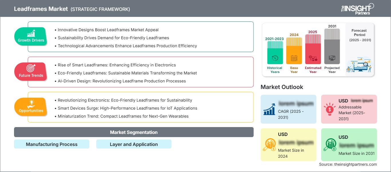
Leadframes Market: Strategic Insights
Regional Insights
North America Leadframes Market
North America represented approximately 18–22% of the Leadframes Market in 2025 and is projected to expand at a CAGR of 11.8–12.6% through 2034. There is investment in the field of semiconductors, auto electronics, industrial automation, and a trend toward resilient supply chains in the region. The US is the main customer, and Canada is a contributor via electronics, industrial, and automotive applications. The expansion of the local semiconductor packaging business may create more demand for locally-qualified suppliers of components.
Reliability, traceability, delivery security, and qualification are becoming increasingly important to regional customers. The automotive applications demand the capability of components to function at tough temperature and voltage conditions, whereas industrial applications seek components’ ruggedness and consistent performance. The expansion of local semiconductor packaging will make it worthwhile to encourage the localization of suppliers, although the APAC region accounts for a large share of leadframe capacity.
U.S. Leadframes Market Market
The Leadframes Market report shows that the US accounted for approximately 72–76% of North American demand in 2025 and is expected to grow at a CAGR of 11.6–12.4% through 2034. Investment in semiconductor ecosystem, automotive electronics, industrial controls, and power device packaging are among the important structural demand generators. Amkor Technology, Inc. offers significant downstream packaging capabilities, and speciality suppliers may be helped by the domestic qualification needs.
There is an increasing need for high-reliability leadframes to provide support for power management, sensing, control devices, and mixed signal devices in the automotive and industrial applications. Investments in US semiconductor packaging capacity can offer better supply resilience and foster long-term procurement relationships. Thermal and electrical efficient QFN, exposed pad, and other packages are among the important demand generators.
Europe Leadframes Market
Europe held an estimated 15–19% share in 2025 and is projected to grow at a CAGR of 12.0–12.8% through 2034. Germany is the foremost regional market due to its automotive and industrial electronics presence. The UK adds demand through aerospace, industrial and technology applications, whereas France gains from automotive, telecommunication and government-sponsored semiconductor activities. Additional demand comes from Italy and Spain through automotive manufacturing, industrial automation and electronics production.
Germany has a special appeal since automotive electrification boosts semiconductors per vehicle content and demands dependable power and control components. Automotive manufacturers require smaller packages with enhanced heat management and quality of surface finish. Also, industrial automation provides a boost to sensor and power management components.
The UK and France offer diversified demand from automotive, telecommunication, aerospace, defense and industrial electronics segments. Italy and Spain derive demand from automotive manufacturing and more general industrial upgrading. In Europe, qualification standards, supply security, energy efficiency and semiconductor manufacturing capacity in the region can stimulate regional supply and local component manufacturing.
APAC Leadframes Market
According to the Leadframes Market forecast, APAC represented approximately 48–52% share in 2025 and is expected to grow at a CAGR of 14.8–15.6% through 2034. The market leaders include China, Japan, South Korea, Taiwan, India, and Australia. The presence of semiconductor packaging ecosystem, electronics fabrication, automobile industry, and industrial policies supports the regional demand for high-quality lead frames.
China has the advantage of electronics and semiconductor capabilities, Japan has advanced materials and packaging capability, and South Korea has semiconductor fabrication capability. India is growing its semiconductor ecosystem, whereas Australia is small in scale yet technically sound. The other applications include automotive electronics, power devices, and telecommunication equipment.
Middle East & Africa Leadframes Market
Middle East & Africa is projected to expand at a CAGR of 9.0–9.8% through 2034. SA and the UAE are the leaders in regional tech investment, whereas South Africa is the main established market for electronics. The Rest-of-MEA market is driven by telecom, industrial machinery, automotive electronics, and developing electronics assembly.
The modernization of infrastructure and energy sector investments generate demand for power management electronics and control systems. There is not much development in semiconductors manufacturing in this region, hence many opportunities are related to import components and technology projects.
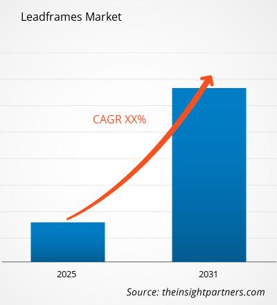
Segmentation Analysis
Type
The Type segment is led by Stamping Process Lead Frame, which is projected to grow at a CAGR of 13.8–14.4% during 2026–2034. Stamping provides high production throughput and repeatability for established package geometries, making it important for high-volume semiconductor assembly. Etching remains strategically relevant where complex, fine-pitch, or customized designs require greater geometric flexibility.
- Stamping Process Lead Frame: Stamping Process Lead Frame supports high-volume semiconductor production through repeatable tooling, rapid cycle times, and established manufacturing economics. It remains important for standardized packages and automotive-scale production.
- Etching Process Lead Frame: Etching Process Lead Frame enables intricate geometries and fine features where mechanical tooling constraints can limit conventional stamping. Its flexibility supports specialized package designs and precision applications.
- Others: Other leadframe approaches address specialized geometries and manufacturing requirements, providing suppliers with flexibility where standard stamping or chemical etching does not fully satisfy package design needs.
Substrate Material
The Substrate Material segment is expected to grow at a CAGR of 13.7–14.3% during 2026–2034. Material selection is determined by electrical conductivity, thermal dissipation, mechanical strength, corrosion resistance, and package reliability. Copper remains dominant, while specialized alloys support applications requiring different mechanical or thermal characteristics.
- Copper: Copper is strategically important because of strong electrical and thermal conductivity, making it suitable for power, automotive, consumer, and general semiconductor packages requiring efficient heat transfer.
- Iron-Nickel Alloy: Iron-Nickel Alloy provides controlled expansion and mechanical characteristics for applications where dimensional stability and compatibility with package materials are important.
- Aluminum: Aluminum supports lightweight and conductivity requirements in selected electronic applications, although package suitability depends strongly on mechanical, thermal, and surface-treatment specifications.
- Others: Other materials serve specialized requirements involving thermal performance, strength, corrosion resistance, or compatibility with particular semiconductor package architectures.
Layer
The Layer segment is projected to register a CAGR of 14.1–14.7% through 2034. Single-layer structures remain important for conventional packaging, while multi-layer configurations are gaining attention where thermal management, electrical routing, and complex package architectures require additional structural functionality.
- Single-Layer: Single-Layer structures remain widely used because they offer established manufacturing processes, straightforward package integration, and cost-effective performance for conventional integrated circuits and discrete semiconductor devices.
- Multi-Layer: Multi-Layer structures provide additional design flexibility and thermal or electrical functionality, supporting specialized packages where conventional single-layer constructions cannot meet performance requirements.
Application
The Application segment is expected to grow at a CAGR of 14.0–14.6% through 2034. Integrated circuits remain central to demand, while discrete devices are gaining importance as electrification and power management increase semiconductor content across automotive and industrial systems.
- Integrated Circuit: Integrated Circuit applications remain strategically important across consumer electronics, automotive controls, telecommunications, industrial systems, and computing equipment requiring reliable semiconductor interconnection.
- Discrete Device: Discrete Device applications benefit from power management, switching, rectification, sensing, and automotive electrification requirements, increasing the need for thermally capable and highly reliable package structures.
- Other: Other applications cover specialized semiconductor devices and package architectures requiring leadframe-based interconnection, thermal management, or compact mechanical integration.
Industry Vertical
The Industry Vertical segment is projected to expand at a CAGR of 14.4–15.0% during 2026–2034. Automotive is positioned as the fastest-growing major vertical because electrification, ADAS, power electronics, sensing, and vehicle computing continue to increase semiconductor requirements per vehicle.
- Automotive: Automotive demand is driven by EV power systems, battery management, sensors, ADAS, infotainment, and electronic control units requiring reliable semiconductor packages.
- Consumer Electronics: Consumer Electronics supports substantial recurring demand through smartphones, appliances, personal devices, and connected equipment requiring compact and cost-efficient semiconductor packaging.
- Telecommunications: Telecommunications applications require semiconductor devices for connectivity, signal processing, power management, and network infrastructure, supporting demand for compact and reliable packages.
- Aerospace & Defense: Aerospace & Defense emphasizes high reliability, environmental resistance, traceability, and long operating life, creating specialized opportunities for qualified semiconductor package components.
- Others: Other industries include industrial automation, energy systems, healthcare electronics, and specialized equipment where semiconductor reliability and thermal performance remain important.
Opportunity Snapshot
| Industry Vertical | Revenue Contribution | Trend Tag | Adoption Stage |
| Automotive | High | EV Power | Scaling |
| Consumer Electronics | High | Device Miniaturization | Mature |
| Telecommunications | Medium | 5G Infrastructure | Scaling |
| Aerospace & Defense | Medium | High Reliability | Emerging |
| Others | Medium | Industrial Controls | Scaling |
Leadframes Market Growth Drivers and Impact Analysis
Rising Semiconductor Content in Electrified Vehicles
Electrification of vehicles has increased the number of semiconductors that are utilized in such vehicles for power conversion, battery management, sensing, controls, and connectivity. There is still a requirement for leadframe packages in many discrete and analog devices due to their proven economics and good thermal paths. With increasing volumes of EVs, the package demands have increasingly been focused on dissipation of heat, reliability of electrical performance, small form factors, and extended qualification timelines. There is an opportunity here for companies that can manufacture exposed pad, power, and fine pitch packages in automotive grade. It is not limited only to passenger cars but also commercial vehicles, chargers, and industrial electrification. Companies that have a strong capability of automotive qualification will get longer programs.
Expansion of Advanced Semiconductor Packaging Capacity
Increasing spending on semiconductor manufacturing and packaging is bolstering the ecosystem around leadframe products. Additional capacity in packaging calls for reliable suppliers of components, which should be able to offer consistency in terms of dimensions, plating performance, materials used, and production volumes. Localization strategies in North America and Europe may present an option to have local technical assistance, dual-sourcing, and shortened supply chains, whereas Asia Pacific will continue offering a strong production scale. Leadframe suppliers may gain from the need of their customers to find additional suppliers to mitigate risks. This becomes especially true for automotive and industrial semiconductors. Increased capacity may stimulate growth in demand not only through increased semiconductor production but also through the need for more robust and localized component supply.
Growth in Power and Analog Semiconductor Applications
Power and analog semiconductors also remain viable for use in various end applications including automotive, industrial, consumer, telecom, and energy infrastructure equipment. Most of these types of semiconductors are packaged in leadframes due to the fact that these packages provide practical electrical connections, physical support, and heat management capabilities while maintaining a cost-effective manufacturing process. As the number of applications requiring regulation, power management, control, sensing, and conditioning of signals increases, so does the leadframe usage, even as more advanced packaging technologies emerge for semiconductors. Semiconductor vendors can seize this opportunity by offering improved heat dissipation, finer pitch capability, better plating, and customized packaging. The potential effect of this market is wide-ranging since the power and analog devices are used in many different types of applications.
Leadframes Market Future Trends
Greater Adoption of Fine-Pitch and Leadless Architectures
The Leadframes Market trends show that future developments in leadframe design are anticipated to include smaller pitch, smaller footprint, exposed pad designs, and leadless configurations that offer improved electrical and thermal characteristics. The use of QFN packages along with other similar packages could provide both reduced package size and effective heat dissipation that makes them good candidates for small automotive, consumer, and industrial applications. Future efforts by manufacturing vendors will be directed towards increased etching precision, advanced stamping technologies, photolithography-based electroplating, and dimensional controls. Such abilities will become more and more necessary since package designers will require higher functional density per chip with no corresponding increase in its physical size. This trend will put the advantage on those manufacturers who will manage to combine precision tooling, surface engineering, automated inspection, and reliable mass production.
Integration of Thermal Management into Leadframe Design
The trends of the Leadframes Market suggest that the future designs will increasingly give more importance to thermal management directly through the leadframes design itself. Die pad exposure, heat slug technology, high-copper alloys, and special surface finish can aid in improved heat dissipation with smaller package sizes. This will be especially important in the automotive power semiconductors, industrial controls, charger ICs and other areas, where the temperature conditions affect the operation of the semiconductor. There will be increased collaboration between the manufacturers of semiconductors and packaging firms at the early stages of design to ensure that material, shape of leads, plating, etc. are designed properly together. The trend might favor custom leadframes over standard ones. The companies with material knowledge combined with manufacturing capabilities should benefit from it.
Leadframes Market Opportunities
Localized Supply for Semiconductor Packaging Ecosystems
Regional semiconductor investment creates opportunities for leadframe suppliers to establish technical centers, finishing operations, or manufacturing partnerships closer to packaging customers. North America and Europe are particularly relevant because expanding semiconductor ecosystems can increase demand for qualified local sources while maintaining links to established Asian production networks. Investment decisions should prioritize automotive and industrial customers where long qualification cycles can support stable programs. Local technical support can reduce development time and improve responsiveness without requiring complete relocation of production. Suppliers can also use regional facilities for inspection, plating, customization, and final processing while retaining large-scale manufacturing in cost-efficient locations. This approach can balance supply-chain resilience with competitive economics and provide a practical pathway into newly developing semiconductor packaging clusters.
Customized Leadframes for Automotive and Power Devices
Customized leadframes offer an opportunity to capture higher-value applications where standard package geometries cannot adequately address thermal, electrical, or mechanical requirements. Automotive power management, EV systems, industrial drives, and charging infrastructure increasingly require packages capable of handling higher power densities and demanding operating environments. Suppliers can invest in application engineering, rapid prototyping, fine-pitch tooling, exposed-pad structures, and advanced surface finishing to support customer-specific designs. Early collaboration with semiconductor packaging companies can improve the probability of design wins because leadframe geometry influences both package performance and assembly efficiency. A customization strategy can also reduce direct price competition by shifting purchasing discussions toward reliability, qualification, lifecycle performance, and engineering support rather than unit cost alone.
Recent Developments
- August 2026: Bruker announced major advances in detector technology, including new high-performance detectors for semiconductor, thin-film, energy-material and nanostructure characterization. The solutions deliver faster data acquisition, higher sensitivity and improved spatial resolution.
- May 2026: Sony Semiconductor Solutions and TSMC entered a preliminary agreement to establish a strategic partnership for next-generation image sensors. The collaboration combines Sony’s image-sensor expertise with TSMC’s advanced manufacturing technology, targeting applications including smartphones, automotive and robotics.
- May 2026: Applied Materials agreed to acquire ASMPT’s NEXX business to strengthen its panel-level advanced packaging portfolio. NEXX’s electrochemical deposition technology will complement Applied’s existing solutions and support larger AI accelerator packages using chiplets and HBM.
Frequently Asked Questions

- Comprehensive Market Sizing and Forecast Analysis
- Detailed Segmentation Analysis
- In-Depth Market Dynamics Assessment
- Regional and Country-Level Insights
- Competitive Landscape and Company Benchmarking
- Strategic Business Intelligence
Recent Reports
Testimonials

The Insight Partners provided valuable market intelligence that supported our global go-to-market strategy. Their team was professional, responsive, and attentive to our feedback, providing thoughtful analysis and helpful methodological clarifications throughout the project.
Junmo Kim Chief Financial Officer (CFO), Enertech Co., Ltd.
The Insight Partners' SCADA System Market report is comprehensive, with valuable insights on current trends and future forecasts. The team was highly professional, responsive, and supportive throughout. We are very satisfied and highly recommend their services.
RAN KEDEM Partner, Reali Technologies LTDs
I requested a report on a very specific software market and the team produced the report in a few days. The information was very relevant and well presented. I then requested some changes and additions to the report. The team was again very responsive and I got the final report in less than a week.
JEAN-HERVE JENN Chairman, Future Analytica
We worked with The Insight Partners for an important market study and forecast. They gave us clear insights into opportunities and risks, which helped shape our plans. Their research was easy to use and based on solid data. It helped us make smart, confident decisions. We highly recommend them.
PIYUSH NAGPAL Sr. Vice President, High Beam Global
The Insight Partners delivered insightful, well-structured market research with strong domain expertise. Their team was professional and responsive throughout. The user-friendly website made accessing industry reports seamless. We highly recommend them for reliable, high-quality research services
YUKIHIKO ADACHI CEO, Deep Blue, LLC.
This is the first time I have purchased a market report from The Insight Partners.While I was unsure at first, I visited their web site and felt more comfortable to take the risk and purchase a market report.I am completely satisfied with the quality of the report and customer service. I had several questions and comments with the initial report, but after a couple of dialogs over email with their analyst I believe I have a report that I can use as input to our strategic planning process.Thank you so much for taking the extra time and making this a positive experience.I will definitely recommend your service to others and you will be my first call when we need further market data.
JOHN SUZUKI President and Chief Executive Officer, Board Director, BK Technologies
I wish to appreciate your support and the professionalism you displayed in the course of attending to my request for information regarding to infectious disease IVD market in Nigeria. I appreciate your patience, your guidance, and the fact that you were willing to offer a discount, which eventually made it possible for us to close a deal. I look forward to engaging The Insight Partners in the future, all thanks to the impression you have created in me as a result of this first encounter.
DR CHIJIOKE ONYIA MANAGING DIRECTOR, PineCrest Healthcare Ltd.Reason to Buy
- Informed Decision-Making
- Understanding Market Dynamics
- Competitive Analysis
- Identifying Emerging Markets
- Customer Insights
- Market Forecasts
- Risk Mitigation
- Boosting Operational Efficiency
- Strategic Planning
- Investment Justification
- Tracking Industry Innovations
- Aligning with Regulatory Trends





 Get Free Sample for