
NEMS (Nano Electro Mechanical Systems) Market Growth, Trends & Demand by 2034
NEMS (Nano Electro Mechanical Systems) Market Size and Forecasts (2021–2034), Global and Regional Share, Trends, and Growth Opportunity Analysis Report Coverage : By Applications (STM/AFM, Medical, Gas/Flow Sensor, RF), Products (Switches, Cantilevers), Components (Nanotubes, Nanowires, Nanofilms), Materials (Graphene, ZnO, SiC, GaN, SiO2)
- Status : Data Released
- Report Code : TIPRE00039551
- Category : Electronics and Semiconductor
- No. of Pages : 150
- Available Report Formats :


- Last update date : October 13, 2026


2025 Market Size
US$ 215.94 Mn
Base year value
2034 Forecast
US$ 1,702.1 Mn
Projected by 2034
CAGR 2026-2034
25.78 %
Growth rate
Addressable Market
US$ 7,248.12 Mn
(2026-2034)
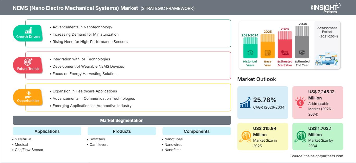
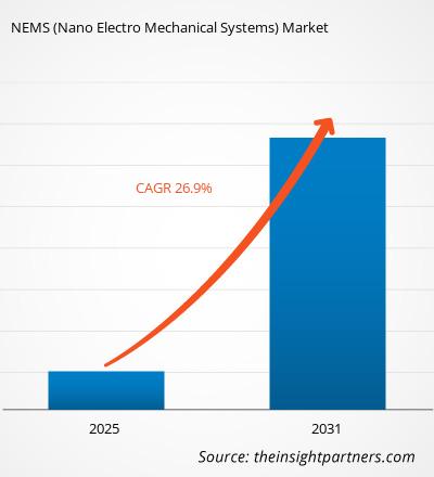
The NEMS Market reached US$ 215.94 Million in 2025 and is projected to reach US$ 1,702.1 Million by 2034, registering a CAGR of 25.78% during 2026–2034. Expansion is fueled by the emergence of nanoscale electromechanical structures with mechanical actuation, electrical detection, and enhanced surface sensitivity. The rise in the use of such technologies in advanced sensing, radio frequency, biomedical sciences, and nanoscale characterization has increased the commercial value of NEMS systems within technology-driven industries.
North America continues to be an important hub for developments in this domain, with the market expected to grow at a CAGR of 25-27% up to 2034. Competent semiconductor research, sophisticated nanofabrication facilities, and consistent investments in sensing solutions have helped drive adoption. The NEMS Market Size is also driven by the incorporation of nanoscale devices in research instruments, medical diagnosis, RF devices, and industrial monitoring equipment.
NEMS (Nano Electro Mechanical Systems) Market Assessment and Insights
- North America: North America is expected to maintain a 34–38% share in 2025 and expand at a 25–27% CAGR between 2026–2034, supported by semiconductor R&D, advanced microscopy, biomedical engineering, and nanoscale fabrication capabilities.
- US: The US represents an estimated 82–86% share of North America in 2025, with growth of 25–27% during 2026–2034, supported by strong research commercialization and advanced instrumentation demand.
- Europe: Europe accounts for an estimated 25–29% share in 2025 and is projected to grow at a 24–26% CAGR through 2034, with Germany, the UK, France, and Italy supporting research, semiconductor, medical, and industrial applications.
- Asia Pacific: Asia Pacific is estimated to hold a 27–31% share in 2025 and grow at a 27–29% CAGR through 2034, led by China, Japan, South Korea, and India through semiconductor expansion and nanotechnology investment.
- Largest Segment: Applications is the largest segment, representing a 32–36% market share in 2025 and expanding at a 26–28% CAGR between 2026–2034.
- High Growth Segment: Medical is the high-growth segment, holding an 18–22% market share in 2025 and advancing at a 29–32% CAGR during 2026–2034.
- Key companies analyzed in detail: Inframat Advanced Materials, LLC; Nanoshell LLC; Sun Innovations, Inc.; CNano Technology Ltd.; Nanocyl SA; Resonac Corporation; Agilent Technologies, Inc.; Oxford Instruments Asylum Research, Inc.; Bruker Corporation; Fraunhofer-Gesellschaft zur Förderung der angewandten Forschung e.V.
Source: The Insight Partners' analysis based on proprietary research, government publications, company annual reports, investor presentations, industry databases, and expert interviews.
NEMS technologies have been evolving through the use of advancements in semiconductor manufacturing processes, nanolithography, thin film deposition, and material science. Architectures are evolving from silicon devices to hybrid systems that combine silicon and other materials such as graphene, nanowires, nanotubes, and films. These changes will help to make devices more resonant, electrically responsive, surface-interacting, and mechanically sensitive. Manufacturing is becoming more connected with wafer-scale manufacturing process and compatibility with current semiconductor manufacturing processes.
The future outlook will be driven by investments in advanced sensing technology, RF miniaturization, biomedical diagnostics, and quantum technology. Asian manufacturing ecosystems are increasing their manufacturing capabilities whereas Europe focuses on energy efficient microsystems and technology transfer to industry. Medical-device and environmental-monitoring related regulatory considerations are also driving application-specific developments. The IMF's 2026 Outlook continues to indicate the unequal nature of worldwide expansion, which underscores the importance of manufacturing economics and geographical diversity of supply chains.
NEMS (Nano Electro Mechanical Systems) Market Report Scope
| Report Attribute | Details |
|---|---|
| Market size in 2025 | US$ 215.94 Million |
| Market Size by 2034 | US$ 1,702.1 Million |
| Global CAGR (2026 - 2034) | 25.78% |
| Historical Data | 2021-2024 |
| Forecast period | 2026-2034 |
NEMS (Nano Electro Mechanical Systems) Market Analysis
Growth drivers of NEMS market include need for sensing systems that offer size reduction, sensitivity improvement, and reduction of power required. Nanoscale mechanical elements are able to sense changes in mass, force, pressure, chemical concentration, or electrical properties. Value chain includes nanomaterials manufacturers, wafer processing vendors, device designers, instrument manufacturers, systems integrators, and research organizations. As far as supply chain, its complexity is caused by technical nature of product, which is dependent on thickness, surface quality, resonance, packaging, and interface issues.
In addition, there are additional capabilities that are provided by such two-dimensional materials as graphene. There are some difficulties connected with transfer, uniformity, adhesion, and reproducibility of such materials. Also, nanotubes and nanowires require morphological and integration issues management. Suppliers that have process knowledge, specialized measurement devices, and research partnerships can overcome qualification hurdles for commercial deployment.
According to the NEMS Market Report, the competitors of the company include instrumentation companies, nanomaterial companies, research organizations, and technology companies. Bruker Corporation and Agilent Technologies, Inc. are valuable because of their ability to perform nanoscale characterization and laboratory technologies. Oxford Instruments Asylum Research, Inc. remains relevant owing to its ability to do atomic force microscopy. Fraunhofer-Gesellschaft zur Förderung der angewandten Forschung e.V. boosts the European research community through its development of applied microsystems and sensors.
More and more investment is flowing into the areas of material integration, automation, high-frequency resonators, biomedical sensing, and semiconductor compatible manufacturing. Simultaneously, Resonac Corporation and Nanocyl SA are providing value by enhancing the wider advanced carbon-materials ecosystem. Inframat Advanced Materials, LLC, Nanoshell LLC, Sun Innovations, Inc., and CNano Technology Ltd. provide capabilities related to nanomaterials. The competition is therefore based on intellectual property, repeatability of fabrication processes, application partnerships, characterization capabilities, and transition from lab to manufacturable architectures.
● REPORT CUSTOMIZATION
Tailor This Report To Align With Your Specific Business Requirements
This report can be customized to align precisely with your business objectives, scope, and target markets. Customization options include tailored segmentation, geography, competitive analysis, and strategic insights to support informed decision-making.
Customize This Report →WHAT YOU CAN ADJUST
- ● Segmentations
- ● Geography
- ● Competitive Analysis
- ● Language Preferences
NEMS (Nano Electro Mechanical Systems) Market: Strategic Insights
Regional Insights
North America NEMS Market
The NEMS Market share of North America is projected to account for 34-38% of the share in 2025 and grow at a 25-27% CAGR until 2034. This region offers benefits from highly concentrated semiconductor research, nanofabrication facilities, cutting-edge microscopy, and existing university-industry cooperation. The United States still leads in demand, driven by research efforts in RF devices, medical diagnostics, sensor applications, and nanomaterials. Canada contributes to growth via nanotechnology research in academia and specific materials.
In addition to this, regional development is driven by rising demand for high-performance sensors in industrial automation and communication. Investments in semiconductor technology are boosting demand for accurate nanoscale characterizations, whereas research in biomedicine is contributing to cantilever-based and resonant sensing solutions. The existing supplier presence in the region helps to accelerate transition from prototypes in laboratories to specific application platforms. Venture and institutional funding in turn contributes to the commercialization of novel nanomaterials and hybrid NEMS constructions.
U.S. NEMS Market
The US holds an estimated share of 82-86% of North America’s 2025 market and will witness a 25-27% CAGR till 2034 due to the presence of high-level semiconductor research & development efforts, advanced research universities, nanotechnology program backed by government, and existing instrumentation capabilities. Organizations like Bruker Corporation, Agilent Technologies, Inc., and Oxford Instruments Asylum Research, Inc. contribute to the overall NEMS industry ecosystem.
Emerging applications include RF switches, advanced microscopes, biological testing, and gas sensing. Graphene resonators, nanowire arrays, and low power transduction are being investigated by research organizations for the future computing and sensing platforms. The ecosystem in the US has the benefit of interaction between universities, national labs, venture-backed technology companies, and instrument companies. This helps in fast material/device concept verification prior to commercialization and hence increases the domestic demand for NEMS components.
Europe NEMS Market
Europe is expected to take a 25–29% market share in 2025 and expand at a 24–26% CAGR up to 2034. The major contributor to Europe’s success will be Germany, thanks to its advanced research and nanotechnology applied in industry. The other countries that offer complementary technologies include the UK, France, Italy, and Spain, covering scientific instrumentation, medical technologies, advanced materials, and semiconductor research.
The UK has good university-based research on nanotechnology and precision instrumentation, used in medical sensors and materials characterization. Germany has a very good industrial base, where applied research contributes to the semiconductor-compatible microsystems, sensors, and advanced materials. France, Italy, and Spain offer increasing capabilities in photonics, industrial automation, aerospace, biomedical engineering, and technology research. Europe’s technology programs now focus more on energy efficiency, miniaturization, and technology transfer, resulting in a continuous flow of NEMS commercialization opportunities.
APAC NEMS Market
APAC has a share of approximately 27-31% in 2025 and is projected to grow at a 27-29% CAGR until 2034, with China being the dominant country. Japan and South Korea offer advanced semiconductor and materials technologies, whereas India and Australia are nurturing opportunities via research.
China provides the electronics manufacturing environment and Japan the technological precision needed for the device fabrication and nanoscale characterization processes. South Korea offers advanced semiconductor and RF technologies, whereas India is nurturing its nanotechnology research and semiconductor manufacturing capabilities. Australia contributes via research conducted by its universities as well as materials science. Industrial policy promoting semiconductor localization, advanced electronics, and scientific research would drive investments in nanomaterials, sensors, and nanoscale electromechanical systems.
Middle East & Africa NEMS Market
Middle East and Africa is expected to register a 22–24% CAGR through 2034. Saudi Arabia and the UAE are building advanced technology and research ecosystems, while South Africa provides established scientific infrastructure. The region's leading opportunities are linked to energy, industrial monitoring, healthcare technology, and advanced infrastructure.
The countries of Saudi Arabia and UAE are stressing technology diversification, smart infrastructures, and advanced manufacturing. The country of South Africa makes contributions through mining, material science, and industrial sensing needs. The rest of the MEA region provides an opportunity where miniature sensors could be used in energy infrastructures, environmental monitoring, and industrial safety. The development of hydrogen and other energy transition activities will further boost the need for gas sensing systems.
Segmentation Analysis
Applications
Applications represent the largest main segment, with a 26–28% CAGR during 2026–2034. The NEMS Market scope across STM/AFM, medical, gas/flow sensing, and RF applications is expanding as device miniaturization improves sensitivity and enables new measurement architectures. Research instrumentation remains foundational, while medical and industrial sensing provide pathways toward higher-volume deployments.
- STM/AFM: STM/AFM applications maintain a strong position because nanoscale imaging and characterization require precise mechanical and electrical interactions. Their strategic importance extends across semiconductor research, advanced materials, graphene studies, and nanofabrication process development.
- Medical: Medical applications are gaining strategic relevance as nanoscale resonators and cantilevers enable highly sensitive analysis of biological interactions, biomarkers, mechanical properties, and molecular events in research and diagnostic environments.
- Gas/Flow Sensor: Gas/Flow Sensor applications address industrial safety, environmental monitoring, process control, and energy infrastructure. Demand is supported by requirements for compact detection architectures capable of responding to low-concentration changes.
- RF: RF applications benefit from nanoscale switching and resonant structures that can support miniaturized high-frequency components. Their strategic value is tied to communications, wireless systems, and future high-frequency electronics.
Products
Products are projected to expand at a 24–26% CAGR through 2034, with switches and cantilevers serving different functional requirements. Switches emphasize electrical control and RF applications, while cantilevers support mechanical sensing, characterization, and biomedical use. Product development is increasingly focused on reliability, repeatability, integration, and compatibility with advanced fabrication processes.
- Switches: Switches address high-frequency and low-power circuit requirements, where compact dimensions and rapid electrical response provide strategic advantages. Demand is connected to communications, RF architectures, and advanced electronic systems requiring configurable signal paths.
- Cantilevers: Cantilevers remain important for mass, force, chemical, and biological sensing. Their established role in atomic force microscopy and nanomechanical measurement supports continued demand across research, diagnostics, materials science, and specialized industrial applications.
Components
Components are expected to register a 27–29% CAGR during 2026–2034. Nanotubes, nanowires, and nanofilms enable device architectures with high surface-to-volume ratios and tunable electrical or mechanical properties. Integration quality remains a key differentiator because defects, dimensional variation, and interface instability can directly affect sensitivity, resonance, and operating lifetime.
- Nanotubes: Nanotubes provide conductive and mechanically robust structures for nanoscale transduction. Their strategic importance stems from high aspect ratios, strong electromechanical characteristics, and compatibility with sensing architectures requiring enhanced surface interaction.
- Nanowires: Nanowires support highly sensitive electrical and mechanical devices because their geometry enables strong response to surface, strain, and environmental changes. They remain important for sensor miniaturization and semiconductor-compatible research.
- Nanofilms: Nanofilms enable thin, functional layers for mechanical, electrical, optical, and chemical transduction. Their importance is increasing where controlled thickness and surface engineering are required to tune resonance, sensitivity, or material compatibility.
Materials
Materials are forecast to grow at a 25–27% CAGR through 2034 as developers seek improved conductivity, mechanical strength, chemical stability, and tunable electromechanical behavior. Graphene, ZnO, SiC, GaN, and SiO2 address distinct performance requirements. Materials selection increasingly depends on fabrication compatibility, environmental stability, and integration economics.
- Graphene: Graphene is strategically important for high-sensitivity NEMS because its atomic thickness, mechanical strength, and electrical properties enable compact transducers and resonators. Its integration remains an active research focus.
- ZnO: ZnO supports piezoelectric and sensing applications where mechanical deformation can be coupled with electrical output. Its material characteristics make it relevant to compact resonators, sensors, and energy-related microsystems.
- SiC: SiC offers mechanical robustness, chemical stability, and high-temperature capability, supporting applications where conventional silicon structures may face environmental or reliability limitations.
- GaN: GaN contributes high-frequency and piezoelectric capabilities, creating opportunities for RF and harsh-environment architectures. Its semiconductor properties also support integration with advanced electronic systems.
- SiO2: SiO2 remains important as an insulating and structural material in nanoscale device fabrication. Its mature processing ecosystem supports repeatable integration into multilayer and semiconductor-compatible architectures.
Opportunity Snapshot
| Applications | Revenue Contribution (High/Medium/Low) | Trend Tag (MAX 2 words) | Adoption Stage (Emerging/Scaling/Mature) |
| STM/AFM | High | Nano Characterization | Mature |
| Medical | Medium | Bio Sensing | Scaling |
| Gas/Flow Sensor | Medium | Trace Detection | Scaling |
| RF | Medium | RF Miniaturization | Emerging |
NEMS (Nano Electro Mechanical Systems) Market Growth Drivers and Impact Analysis
Demand for high-sensitivity miniaturized sensing architectures
Demand for nanoscale sensing is increasing as manufacturers seek smaller devices capable of detecting weak mechanical, chemical, electrical, and biological signals. NEMS architectures can exploit high surface-to-volume ratios and resonant behavior to improve detection performance while reducing physical footprint. This advantage is relevant to semiconductor metrology, industrial monitoring, medical research, and environmental applications. The impact is strongest where conventional sensors face limitations in sensitivity, size, or power consumption. As connected equipment becomes more distributed, compact sensing nodes can support localized monitoring and faster response. The resulting commercial effect extends beyond individual devices because higher sensitivity can reduce sample requirements, improve measurement precision, and enable earlier detection of changes in industrial or biological systems.
Expansion of advanced semiconductor and nanofabrication ecosystems
Investment in semiconductor manufacturing and advanced fabrication infrastructure is creating a favorable technology environment for nanoscale electromechanical systems. Wafer-scale processing, thin-film deposition, lithography, and advanced packaging can support repeatable fabrication of increasingly complex structures. The IEA expects global data-center electricity consumption to roughly double from 2025 to 2030, increasing pressure for efficient computing and sensing technologies. NEMS can contribute indirectly through low-power switching, monitoring, and nanoscale characterization. The market impact is therefore linked to both device production and the measurement infrastructure required to qualify advanced chips and materials. As fabrication ecosystems mature, suppliers able to deliver reliable nanoscale components and compatible characterization workflows can address a broader range of industrial customers.
Growing integration of nanomaterials into electromechanical devices
The development of graphene, nanotubes, nanowires, and engineered thin films is widening the performance envelope available to NEMS designers. Graphene is particularly relevant because its combination of mechanical strength, electrical conductivity, and atomic-scale thickness enables compact resonators and transducers. Research published in 2025 demonstrated continued progress in graphene-enabled silicon NEMS architectures and electrically tunable nanomechanical resonators. These developments can improve frequency control, sensitivity, and multifunctionality. Commercial impact will depend on overcoming material transfer, uniformity, contact resistance, packaging, and large-scale manufacturing challenges. Companies that establish repeatable integration processes can potentially move advanced materials from laboratory demonstrations into specialized sensor, RF, and instrumentation products.
NEMS (Nano Electro Mechanical Systems) Market Future Trends
AI-assisted nanoscale measurement and adaptive sensing
NEMS Market trends are moving toward measurement systems that combine nanoscale sensing with AI-assisted interpretation, automated calibration, and adaptive control. Instead of treating the sensor and analytical system as separate elements, future architectures are likely to integrate signal processing closer to the transducer. This approach can reduce data movement, improve response time, and support continuous monitoring. AI-enabled analysis can also compensate for environmental drift, identify anomalies, and optimize operating parameters dynamically. The opportunity is particularly relevant to semiconductor inspection, biomedical research, and industrial gas monitoring. As sensor networks become more distributed, edge processing may become increasingly important for minimizing power consumption and communication requirements while retaining high-frequency or high-resolution measurement capability.
Hybrid two-dimensional material architectures
Future devices are likely to combine established silicon structures with graphene and other two-dimensional materials rather than replacing conventional substrates entirely. Hybrid architectures can provide mechanical stability from established materials while adding electrical tunability, high sensitivity, or specialized surface functionality. Recent research has demonstrated growing interest in graphene-integrated MEMS and NEMS structures, including suspended membranes and electrically controlled resonators. This direction could support multifunctional sensors capable of measuring mechanical, electrical, chemical, or biological signals within compact platforms. Commercial progress will depend on repeatable transfer processes, scalable patterning, robust contacts, and reliable packaging. The trend therefore favors suppliers that can combine nanomaterial expertise with semiconductor-compatible fabrication and characterization.
NEMS (Nano Electro Mechanical Systems) Market Opportunities
Commercialization of medical and biomedical nanomechanical sensing
NEMS Market Forecasts indicate attractive strategic potential in medical and biomedical sensing as researchers seek compact platforms capable of detecting molecular interactions, biomarkers, mechanical properties, and cellular responses. Investment opportunities exist across specialized diagnostic instruments, research tools, drug-development workflows, and point-of-care technologies. The WHO's recent medical-device policy work emphasizes stronger frameworks for digital health, diagnostics, sustainability, and health-technology management, creating a clearer environment for technology assessment. Investors and manufacturers can prioritize partnerships with hospitals, universities, and diagnostic developers to validate performance in clinically relevant settings. Commercial success will depend on analytical accuracy, reproducibility, regulatory evidence, manufacturability, and integration with established diagnostic workflows.
Low-power RF and industrial sensing platforms
A second opportunity lies in integrating NEMS structures into RF components and industrial monitoring platforms where size, frequency response, and energy efficiency influence system design. Semiconductor localization programs in Asia, advanced electronics investment in North America, and European emphasis on industrial digitalization can support demand for specialized components. Opportunities are particularly relevant to high-frequency switching, compact resonators, gas detection, and infrastructure monitoring. Developers can strengthen market access by designing components around existing fabrication processes rather than relying entirely on proprietary manufacturing. Strategic partnerships with semiconductor foundries, instrumentation providers, and system integrators can also shorten qualification cycles and reduce the commercial risk associated with moving from laboratory prototypes to repeatable production.
Frequently Asked Questions

- Comprehensive Market Sizing and Forecast Analysis
- Detailed Segmentation Analysis
- In-Depth Market Dynamics Assessment
- Regional and Country-Level Insights
- Competitive Landscape and Company Benchmarking
- Strategic Business Intelligence
Recent Reports
Testimonials

The Insight Partners provided valuable market intelligence that supported our global go-to-market strategy. Their team was professional, responsive, and attentive to our feedback, providing thoughtful analysis and helpful methodological clarifications throughout the project.
Junmo Kim Chief Financial Officer (CFO), Enertech Co., Ltd.
The Insight Partners' SCADA System Market report is comprehensive, with valuable insights on current trends and future forecasts. The team was highly professional, responsive, and supportive throughout. We are very satisfied and highly recommend their services.
RAN KEDEM Partner, Reali Technologies LTDs
I requested a report on a very specific software market and the team produced the report in a few days. The information was very relevant and well presented. I then requested some changes and additions to the report. The team was again very responsive and I got the final report in less than a week.
JEAN-HERVE JENN Chairman, Future Analytica
We worked with The Insight Partners for an important market study and forecast. They gave us clear insights into opportunities and risks, which helped shape our plans. Their research was easy to use and based on solid data. It helped us make smart, confident decisions. We highly recommend them.
PIYUSH NAGPAL Sr. Vice President, High Beam Global
The Insight Partners delivered insightful, well-structured market research with strong domain expertise. Their team was professional and responsive throughout. The user-friendly website made accessing industry reports seamless. We highly recommend them for reliable, high-quality research services
YUKIHIKO ADACHI CEO, Deep Blue, LLC.
This is the first time I have purchased a market report from The Insight Partners.While I was unsure at first, I visited their web site and felt more comfortable to take the risk and purchase a market report.I am completely satisfied with the quality of the report and customer service. I had several questions and comments with the initial report, but after a couple of dialogs over email with their analyst I believe I have a report that I can use as input to our strategic planning process.Thank you so much for taking the extra time and making this a positive experience.I will definitely recommend your service to others and you will be my first call when we need further market data.
JOHN SUZUKI President and Chief Executive Officer, Board Director, BK Technologies
I wish to appreciate your support and the professionalism you displayed in the course of attending to my request for information regarding to infectious disease IVD market in Nigeria. I appreciate your patience, your guidance, and the fact that you were willing to offer a discount, which eventually made it possible for us to close a deal. I look forward to engaging The Insight Partners in the future, all thanks to the impression you have created in me as a result of this first encounter.
DR CHIJIOKE ONYIA MANAGING DIRECTOR, PineCrest Healthcare Ltd.Reason to Buy
- Informed Decision-Making
- Understanding Market Dynamics
- Competitive Analysis
- Identifying Emerging Markets
- Customer Insights
- Market Forecasts
- Risk Mitigation
- Boosting Operational Efficiency
- Strategic Planning
- Investment Justification
- Tracking Industry Innovations
- Aligning with Regulatory Trends





 Get Free Sample for